这篇文章基于PCIM欧洲2024,一解决超大规模数据中心中采用的尖端处理器不断增长的功率需求,特别是用于训练大型人工智能模型。从交流/DC电源到直接位于处理器旁边的负载点(POL)功率级,不断增长的功率要求给整个功率转换链带来了巨大的挑战。
This article is based on PCIM Europe 2024, which addresses the growing power needs of cutting-edge processors used in hyperscale data centers, especially for training large AI models. From the AC /DC power supply to the Point of load (POL) power stage located directly next to the processor, the growing power requirements present a significant challenge for the entire power conversion chain.
生成式人工智能的崛起及其电力需求
The rise of generative artificial intelligence and the demand for electricity
能够根据预先配置的模型创建数据的生成式人工智能的出现,推动了服务器安装量的大幅增长。诸如ChatGPT、微软的Copilot和具有大量参数的大型语言模型之类的新应用需要越来越强大的处理器来有效地训练这些模型。
The emergence of generative AI, which is able to create data from pre-configured models, has driven a huge increase in server installations. New applications such as ChatGPT, Microsoft's Copilot, and large language models with a large number of parameters require increasingly powerful processors to effectively train these models.
这种从传统串行数据处理的转变,正如在x86处理器的经典冯诺依曼架构中所看到的,需要范式的改变。现代的人工智能训练在很大程度上依赖于大规模并行计算,利用图形处理单元(GPU)和张量处理单元(TPU)等架构。这些处理器拥有数百个内核和高带宽存储器,要么单片集成,要么使用一种称为基片上芯片(CoWoS)的技术在同一封装内横向排列为堆叠的芯片。
This shift away from traditional serial data processing, as seen in theic von Neumann architecture of x86 processors, requires a paradigm change. Modern AI training relies heavily on massively parallel computing, utilizing architectures such as graphics processing units (Gpus) and tensor processing units (Tpus). These processors, with hundreds of cores and high-bandwidth memory, are either integrated on a single chip or arranged laterally into stacked chips within the same package using a technology called chip on a Substrate (CoWoS).
此外,小芯片技术和用于将标线限制的管芯连接成更大的“超级芯片”的方法的进步正在推动这些系统的计算能力的指数增长。随着电力线成为进一步扩展的瓶颈逻辑晶体管的未来在于通过位于处理器背面的埋置电源线供电,通过纳米硅通孔连接到正面。
In addition, advances in small chip technology and methods for connecting wired limited tube cores into larger "superchips" are driving exponential growth in the computing power of these systems. As power lines become a bottleneck for further expansion the future of logic transistors lies in being powered through a buried power cord located on the back of the processor, connected to the front through a nanoparticle silicon through-hole.
这些进步的结果是在负载电流和瞬态响应方面处理器功率需求的急剧增加。电源电压约为0.7 V时,每个处理器的功耗超过1 kW,相当于负载电流超过1,500 A。
The result of these advances is a dramatic increase in processor power requirements in terms of load current and transient response. At A supply voltage of about 0.7 V, each processor consumes more than 1 kW, which corresponds to a load current of more than 1,500 A.
反思权力传递:从横向到纵向
Rethinking power transfer: from horizontal to vertical
基于分立功率级和独立电感的传统横向功率传输难以应对现代处理器过高的电流需求。与这种方法相关的配电损耗与负载电流的平方成比例,随着每一代新一代日益耗电的处理器,情况越来越糟。因此,电力输送需要垂直重新设计,如图1所示。
Traditional transverse power transmission based on discrete power stages and independent inductors is difficult to cope with the excessive current demand of modern processors. The distribution losses associated with this approach are proportional to the square of the load current and get worse with each new generation of increasingly power-hungry processors. As a result, power delivery requires a vertical redesign, as shown in Figure 1.
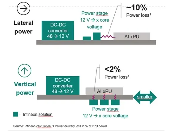
图1:在12v至内核的功率转换过程垂直功率流显著降低功率损耗
Figure 1: Vertical power flow significantly reduces power loss during 12v to core power conversion
由于空间限制,将功率级、栅极驱动器和电感器异构3D集成到紧凑的DC模块中是必不可少的。虽然传统解决方案通常直接通过电感冷却功率级,但这需要通过模块路由所有主板输入信号,从而使3D设置变得复杂。
Due to space constraints, integrating the power stages, gate drivers, and inductor heterogeneous 3D into a compact DC module is essential. While traditional solutions typically cool the power stages directly through inductors, this requires routing all motherboard input signals through modules, which complicates 3D setup.
英飞凌科技公司采取了独特的方法,选择通过电感冷却功率级。此外,它使用了一种新型磁性材料,具有低铁损和软饱和特性,与竞争解决方案相比,效率提高了2%。
Infineon Technologies has taken a unique approach by choosing to cool the power stages through inductors. In addition, it uses a new type of magnetic material with low iron loss and soft saturation properties, which improves efficiency by 2% compared to competing solutions.
图2显示了英飞凌的TDM22544D和TDM22545D双相模块,封装在一个紧凑的9×10mm2尺寸小,峰值电流高达160 A。这些模块有两种高度,5毫米和8毫米,以满足各种空间限制。
Figure 2 shows Infineon's TDM22544D and TDM22545D biphase modules, packaged in A compact 9 x 10mm2 size with a peak current of up to 160 A. These modules are available in two heights, 5 mm and 8 mm, to meet various space constraints.
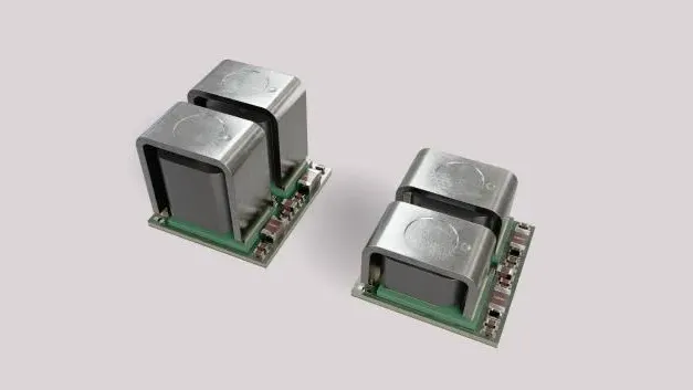
图2:英飞凌的垂直背面模块
Figure 2: Vertical rear module of Infineon
中间总线转换器的作用
The role of the intermediate bus converter
中间总线转换器(IBC)充当机架背板提供的48 V电压和POL级电压之间的媒介。输入电压可以在40至60 V之间变化,也可以严格调节至50 V,如当前发布的Open Compute Spec v3.0所规定。
The intermediate Bus Converter (IBC) acts as a medium between the 48 V voltage provided by the rack backplane and the POL level voltage. The input voltage can vary between 40 and 60 V, or it can be strictly regulated to 50 V, as specified in the currently released Open Compute Spec v3.0.
IBC输出的最佳电压水平需要仔细考虑,以平衡IBC和POL级之间的功率分配损耗,并针对POL级内的开关损耗为处理器供电。较低的中间总线电压允许pol以较高的开关频率(1 MHz或更高)工作,并使用较低额定功率的MOSFETs,如15V型号。
The optimal voltage level for the IBC output needs to be carefully considered to balance power distribution losses between the IBC and POL stages and to power the processor against switching losses within the POL stage. The lower intermediate bus voltage allows the pol to operate at a higher switching frequency (1 MHz or higher) and use lower power ratings of MOSFETs, such as 15V models.
最近的一项分析发表在亚太经合组织2024英特尔和谷歌提出,中间总线电压为8 V的6:1分压器对于电阻在3到6mω之间的配电网络最为有效。GPU或TPU等加速卡的配电电阻通常低于1mω,可以使用8:1分压器为40至60V输入产生5至7.5 V的中间总线电压。
A recent analysis published at APEC 2024 by Intel and Google proposes that a 6:1 divider with an intermediate bus voltage of 8 V is most effective for distribution networks with resistances between 3 and 6mω. Acceleration cards such as Gpus or Tpus typically have distribution resistances below 1mω and can generate intermediate bus voltages of 5 to 7.5V for 40 to 60V inputs using 8:1 dividers.
此时,8:1比率的纯电容分压器过于昂贵且占用空间大,而基于变压器的LLC功率级提供了一种选择。混合开关电容转换器结合了电容和基于变压器的功率传输,是英飞凌提出的解决方案。
At this point, the 8:1 ratio of pure capacitance dividers is too expensive and takes up too much space, and the transformer-based LLC power stage provides an option. Hybrid switched capacitor converters, which combine capacitors and transformer-based power transmission, are the solution proposed by Infineon.
反思备用电源:从UPS到48v电池集成
Rethinking backup power: from UPS to 48v battery integration
大型云服务提供商越来越多地放弃传统上与主配电串联的不间断电源(ups)。这些具有双重交流/DC和DC/交流转换的UPS系统,在数据中心的总功率流中会导致4%到6%的效率损失,大大增加了运营支出成本。
Large cloud service providers are increasingly moving away from uninterruptible power supplies (UPSs) that are traditionally connected in series to the main distribution. These UPS systems, with dual AC /DC and DC/ AC conversions, result in efficiency losses of 4 to 6 percent of the total power flow in the data center, significantly increasing the cost of operating expenses.
现代备用电源解决方案在48v DC水平下并行运行,利用位于同一机架或附近专用于计算托盘的机架中的锂离子(Li-ion)电池。开放计算规范规定,备用电池单元的输出电压调节至48 V。一个双向DC/DC转换器位于锂离子电池和连接到IBC的48V供电轨之间。
Modern backup power solutions operate in parallel at the 48v DC level, utilizing lithium-ion (Li-ion) batteries located in the same rack or nearby racks dedicated to computing trays. The open computing specification stipulates that the output voltage of the standby battery unit is adjusted to 48 V. A bi-directional DC/DC converter is located between the lithium-ion battery and the 48V supply rail connected to the IBC.
通过串联和并联连接,锂离子电池的电池电压范围可以选择以48 V为中心,而不是处理整个电池组的功率。对于完全调节的48v输出,这种方法只需要处理一小部分功率。
With series and parallel connections, the battery voltage range of the lithium-ion battery can be chosen to be centered around 48 V, rather than dealing with the power of the entire battery pack. For a fully regulated 48v output, this method only needs to handle a small fraction of the power.
英飞凌科技的一个系统在电池电压范围的中点达到了99.6%的峰值效率,如图3所示。如图4所示,该系统使用谐振频率LLC转换器和降压转换器进行调节。为了提供48 V电压,电路会调整锂离子电池组电压的极性,该电压可以是正的,也可以是负的。
One system from Infineon Technologies achieved peak efficiency of 99.6% at the midpoint of the battery voltage range, as shown in Figure 3. As shown in Figure 4, the system is tuned using a resonant frequency LLC converter and a buck converter. To provide a 48-V voltage, the circuit adjusts the polarity of the lithium-ion battery pack voltage, which can be either positive or negative.
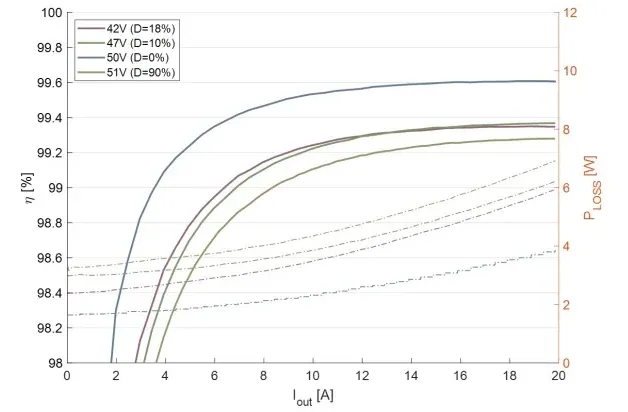
图3:部分功率转换器的实测效率曲线
Figure 3: Measured efficiency curves of some power converters

图4:部分功率转换器的拓扑结构
Figure 4: Topology of a partial power converter
高密度、高效率的交流/DC电源
High density, high efficiency AC /DC power supply
随着计算机架功率水平持续上升,电源架的数量或服务器电源的额定值都必须相应调整。对于训练AI模型,已建立的3千瓦交流/DC电源单元(PSU)可能很快会被额定功率为5.5千瓦的PSU取代。未来的发展可能会将这些功率水平提高到8千瓦,并有可能超过每台单相PSU 10千瓦。
As computer rack power levels continue to rise, the number of power racks or the rating of server power supplies must be adjusted accordingly. For training AI models, the established 3 kW AC /DC power unit (PSU) may soon be replaced by a PSU rated at 5.5 kW. Future developments could increase these power levels to 8 kW and potentially exceed 10 kW per single-phase PSU.
由于效率对电力成本和消耗的直接影响,因此效率仍然是一个关键问题,这些电源必须同时实现非常高的功率密度(高达100 W/in。3)和卓越的效率(高达97.5%)。
Efficiency remains a key issue due to its direct impact on the cost and consumption of electricity, and these power supplies must simultaneously achieve very high power densities (up to 100 W/in). 3) and excellent efficiency (up to 97.5%).
在这种情况下,采用基于碳化硅或氮化镓的宽带隙(WBG)功率器件是一种明确的解决方案。图腾柱功率因数校正(PFC)电路利用碳化硅MOSFETs和工作在高开关频率的DC/DC级是许多设计人员的首选,利用GaN HEMTs提供的有利品质因数和低稀有DS(开)×Q航天科学局产品和零反向恢复费用。
In this case, a silicon carbide or gallium nitride based wideband gap (WBG) power device is a clear solution. Totem pole power factor correction (PFC) circuits utilizing silicon carbide MOSFETs and DC/DC stages operating at high switching frequencies are preferred by many designers, taking advantage of the favorable quality factor and low rarity DS(on)×Q NASA products offered by GaN HEMTs and zero reverse recovery costs.
另一种有前途的方法是使用多级拓扑进行PFC。英飞凌科技公司最近展示了一种三级飞跨电容PFC级,在功率密度超过one hundred and fifty瓦/英寸的情况下,效率达到99.2%。3。
Another promising approach is to use a multilevel topology for PFC. Infineon Technologies recently demonstrated a three-stage flying transcapacitor PFC stage that achieves 99.2% efficiency at power densities of more than one hundred and fifty watts per inch. 3.
这一概念基于即将推出的额定电压为400的SiC MOSFET。此外,采用专有电路来有效地利用存储在电解电容器单元内的几乎全部能量,同时保持DC/DC转换器的恒定输入电压。
The concept is based on the upcoming SiC MOSFETs with a voltage rating of 400. In addition, proprietary circuitry is employed to efficiently utilize almost all of the energy stored within the electrolytic capacitor cell while maintaining a constant input voltage to the DC/DC converter.
现代处理器的巨大功率需求使得整个功率转换链都需要创新的解决方案。需要垂直背面电源模块来处理不断增加的处理器电流,而输出电压在6至8 V之间的IBC在POL级提供了配电损耗和开关损耗之间的平衡。
The enormous power demands of modern processors require innovative solutions along the entire power conversion chain. A vertical rear PSU is required to handle the increasing processor current, while an IBC with an output voltage between 6 and 8 V provides a balance between distribution losses and switching losses at the POL level.
部分电源转换器可在交流电源断电时提供可靠的备用电源解决方案。同时,交流/DC电源可以从多级架构和最新的WBG基于的电源设备。
Some power converters provide a reliable backup power solution in the event of a loss of AC power. At the same time, AC /DC power supplies are available from multi-level architectures and the latest WBG based power devices.